Electronic Analysis of CMOS Logic Gates — Quiz-2 Master Guide
Textbook: J.P. Uyemura, Introduction to VLSI Circuits and Systems, Chapter 7 (7.1–7.11). This guide teaches every section exactly as derived in the book, with equation numbers (7.x), textbook page figures, and a numerical after every topic.
⚠️ Syllabus confusion cleared: your pasted list (7.1 Structured Procedures, D-Latch, JK-FF, MUX…) is Verilog-HDL Chapter 7 (lab / HDL topic), NOT this quiz. Quiz-2 per Course Plan (Lec 20–28) + the image you sent = Uyemura Ch.7 CMOS analysis. This guide covers Uyemura Ch.7 fully, + a 1-page topology-only primer of pre-midterm slides (low weightage) as you asked.
📌 Quiz scope & mark strategy
Course Plan 23ECE302 · Lectures 20–28 · CO2/CO3
| Lecture | Topic (Course Plan wording) | Book section | Likely Q |
|---|---|---|---|
| 20–21 | DC switching characteristics of CMOS inverter — VTC, noise margins | 7.1 | VM numerical (Eq 7.14), VOH/VOL, NML/NMH — almost guaranteed 1Q |
| 22–24 | DC characteristics of NAND and NOR | 7.4 | Simultaneous-switching VM (7.94/7.97), left/right shift reason |
| 25–27 | Transient response of inverter — rise/fall, delay | 7.2 + 7.5 | Rn/Rp → tr/tf → fmax/tp; worst-case NAND/NOR — biggest marks |
| 28 | Power dissipation | 7.3 | Pdyn = C·V²·f, PDC — 1 short numerical |
| 29–31 (spill) | Gate design for transient performance | 7.7 (book) / Ch.8 start | Sizing: series n×, parallel 1× |
⏱️ 60-minute fast path (if quiz is tomorrow)
Do in this order. Tick as you go.
- 15 min — §7.1: memorise Eq 7.14 (VM) + do Solved 7.1A below. Understand βn/βp → VM shift.
- 15 min — §7.2: memorise Rn/Rp (7.28), tr/tf=2.2τ, tp=0.69τ. Do Solved 7.2A (Ex 7.3 style).
- 10 min — §7.3: Pdyn=C·V²·f. Do 1 power sum.
- 10 min — §7.4 + 7.7: NAND shifts right (×1/N), NOR shifts left (×N); sizing series n×.
- 10 min — Read formula sheet aloud twice + attempt 2 unsolved in bank.
🧩 Primer: pre-midterm slides — topology only (low weightage)
Cover "topologically" as requested. One line each — enough for 1-mark questions.
- Ch.1–2: CMOS inverter = pFET pull-up to VDD + nFET pull-down to GND. NAND = parallel p + series n. NOR = series p + parallel n. TG = n+p in parallel. Pass FET = single FET, suffers threshold drop.
- Ch.3: Stick diagram / Euler path — just know pull-up vs pull-down duality; DRC = spacing/width rules (no numerical in Quiz-2).
- Ch.6 (needed for Ch.7!): Square-law ID = (β/2)(VGS−VT)² (saturation, λ=0). β=k′(W/L), k′=μCox. FET RC model: ON FET ≈ resistor R=1/[β(VDD−VT)]; drain cap Cdb=Cj·Area+Cjsw·Perim. Elmore: series Rs add, internal caps add extra R·C term. If you know these 3, Ch.7 derivations click.
- Verilog Ch.7 list you pasted (procedural assignments, D-latch/FF, JK-FF, counter, MUX/casex, loops) — not in this quiz; keep for lab/MH. If a 1-mark HDL Q sneaks in: blocking (=) vs non-blocking (<=), synchronous vs async clear, case vs casex (don't-cares) — that's all.
7.1 DC Characteristics of the CMOS Inverter (pp.237–244)
Book derivation exactly. Core = VTC + VM.
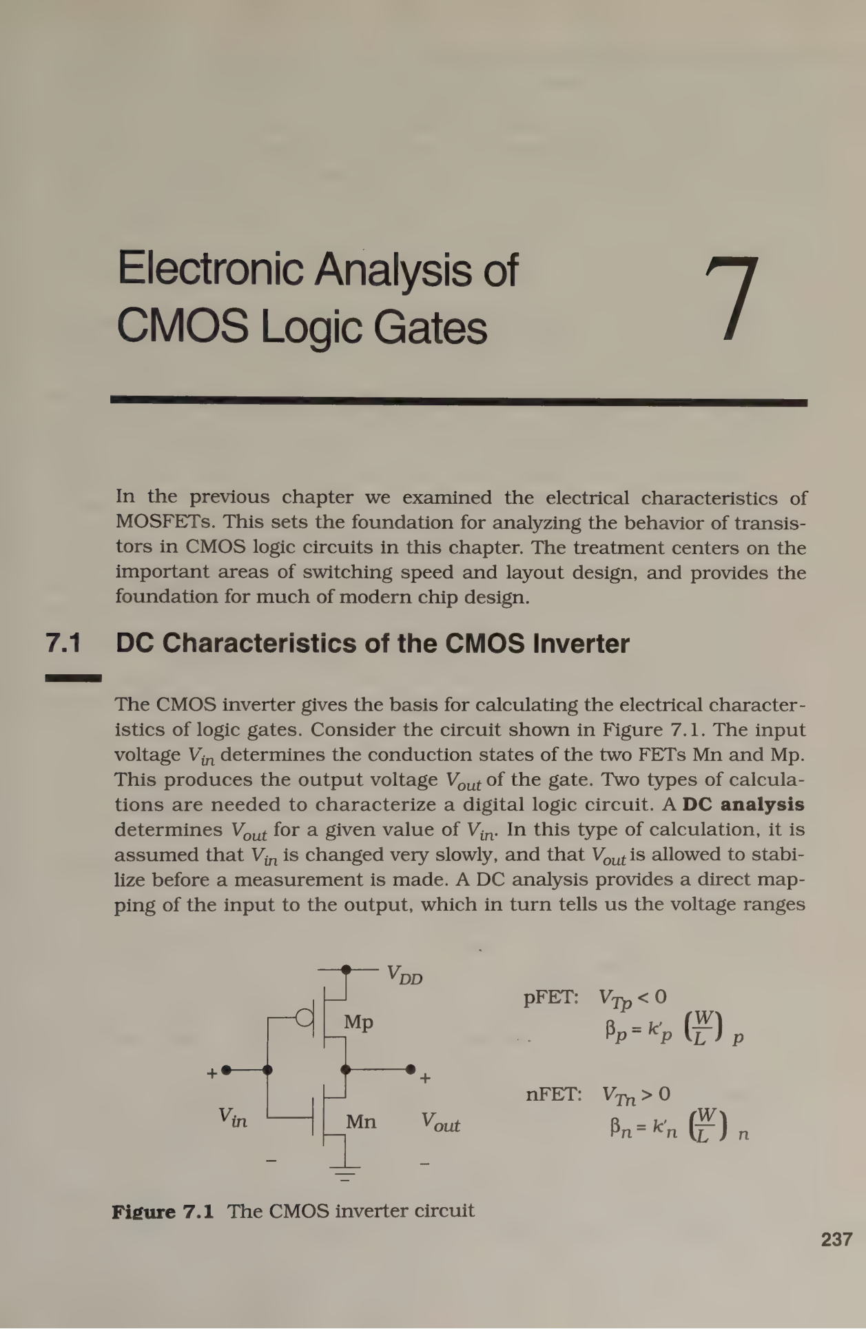
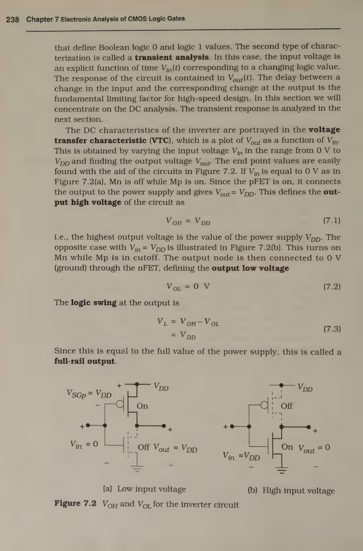
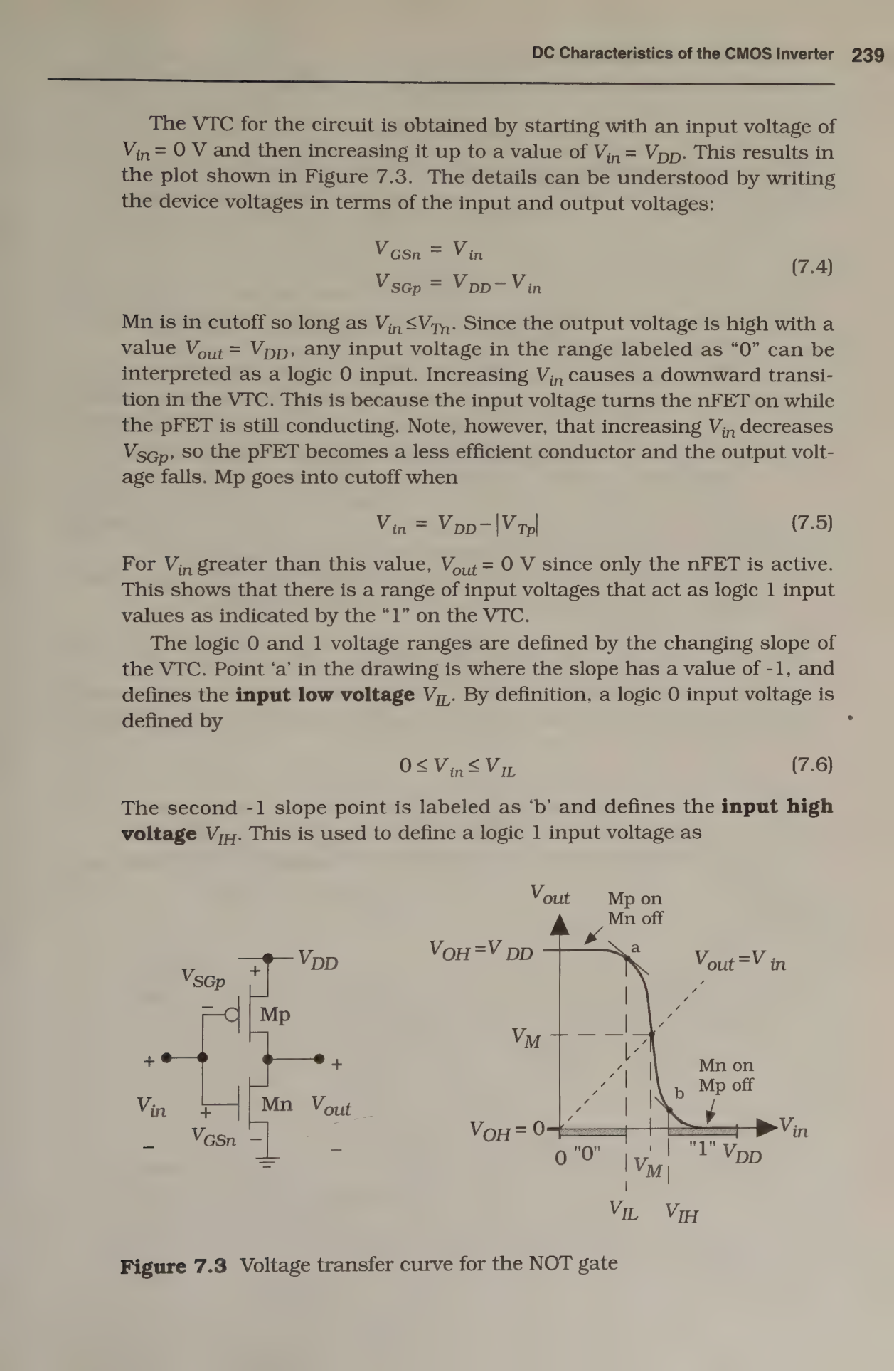
Story in 4 lines
Slowly sweep Vin 0→VDD, record Vout → VTC. Ends are full-rail (CMOS superpower). Middle has two unity-gain points (slope −1) that define legal 0/1 input ranges and noise margins. The crossing with Vout=Vin line is VM (switching threshold) — set by βn/βp.
VOL = 0 V (7.2)
VL = VOH−VOL = VDD (full rail) (7.3)
VGSn=Vin ; VSGp=VDD−Vin (7.4)
pFET cuts off when Vin=VDD−|VTp| (7.5)
NML=VIL−VOL ; NMH=VOH−VIH (7.8)
1. Set Vin=Vout=VM. KCL: IDn=IDp (7.9)
2. Prove both saturated: VDSn=VM > Vsat=VM−VTn (since VTn>0) (7.10–7.11). Same for pFET.
3. Square-law (λ=0): (βn/2)(VM−VTn)² = (βp/2)(VDD−VM−|VTp|)² (7.12)
4. √both sides: √(βn/βp)·(VM−VTn) = VDD−VM−|VTp| (7.13)
5. Solve linear eq for VM:
βn/βp = [k′n(W/L)n]/[k′p(W/L)p] (7.15) · k′n/k′p = 2–3 (7.16)
Symmetric VM=VDD/2 needs βn=βp (if VTn=|VTp|) (7.18–7.20) → (W/L)p/(W/L)n = k′n/k′p ≈ 2.33
✅ Solved 7.1A — Ex 7.1 style (do this first)
Given: k′n=140, k′p=60 µA/V², VTn=0.7, |VTp|=0.7, VDD=3.0 V.
(a) Size for symmetric: need βn=βp → (W/L)p/(W/L)n = 140/60 = 2.33. So Wp≈2.33·Wn (same L). Then VM=VDD/2=1.50 V.
(b) Same sizes (W/L)p=(W/L)n: βn/βp=2.33, √=1.527. VM=(3.0−0.7+1.527·0.7)/(1+1.527)=(2.30+1.069)/2.527=≈1.33 V < 1.5 V. ✓ left shift.
(c) VOH=3.0, VOL=0, swing=3.0 V full rail.
✏️ Try yourself 7.1B (Problem [7.1])
k′n=100, VTn=0.70, k′p=42, VTp=−0.60, VDD=3.3, (W/L)n=10, (W/L)p=14. Find VM. Hint: βn=100·10=1000, βp=42·14=588, ratio=1.70, √=1.304 → VM≈?
Answer (verify): ≈1.42 V. Steps: (3.3−0.6+1.304·0.7)/(1+1.304)=(2.7+0.913)/2.304=3.613/2.304=1.568? Recompute carefully — see trap: |VTp|=0.6. (3.3−0.6=2.7). 2.7+0.913=3.613/2.304=1.57 V. (Recheck arithmetic in exam!)
7.2 Inverter Switching Characteristics (pp.244–257) — highest marks
RC model → exponential → tr/tf/tp. Memorise the chain.
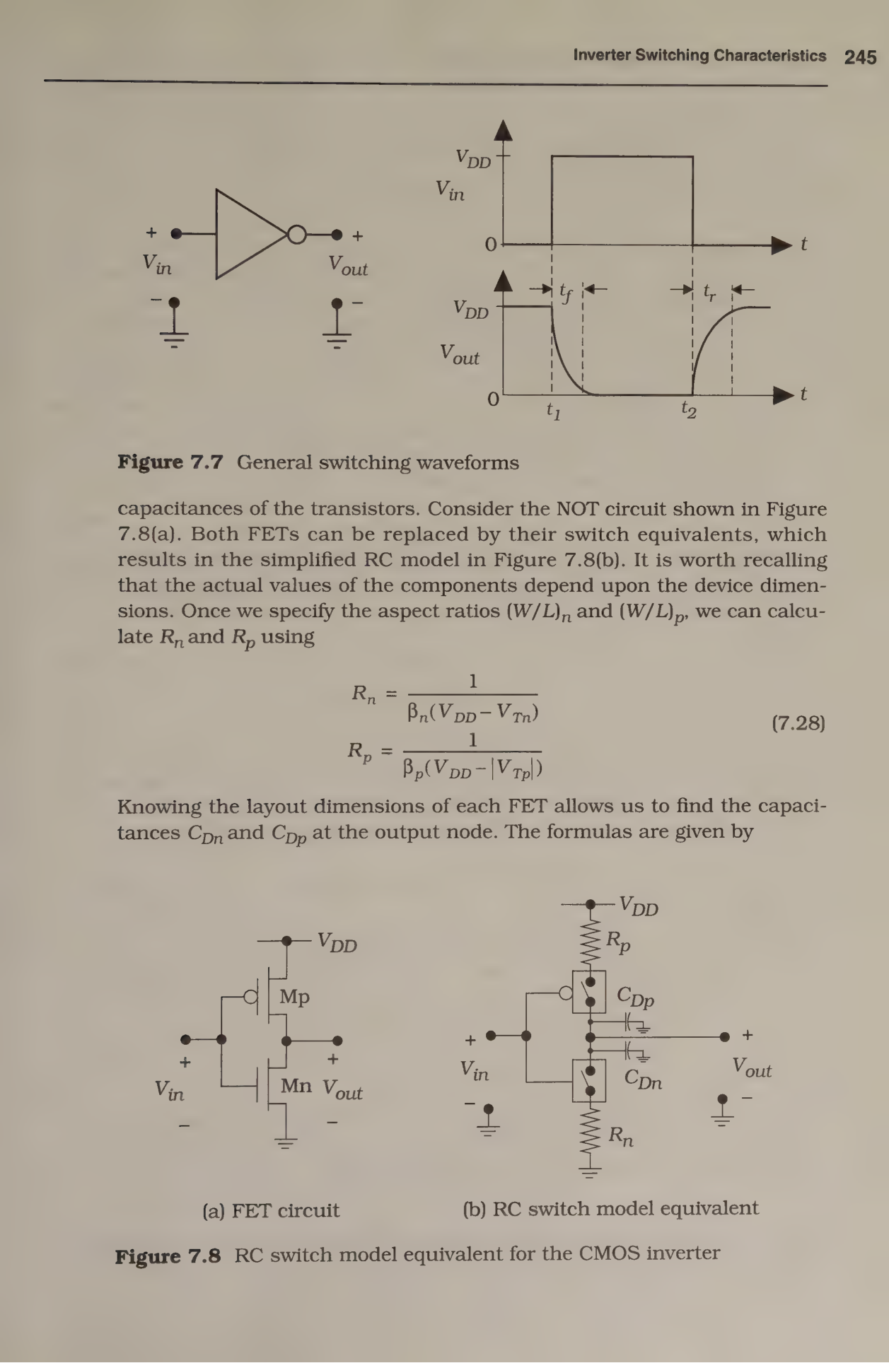
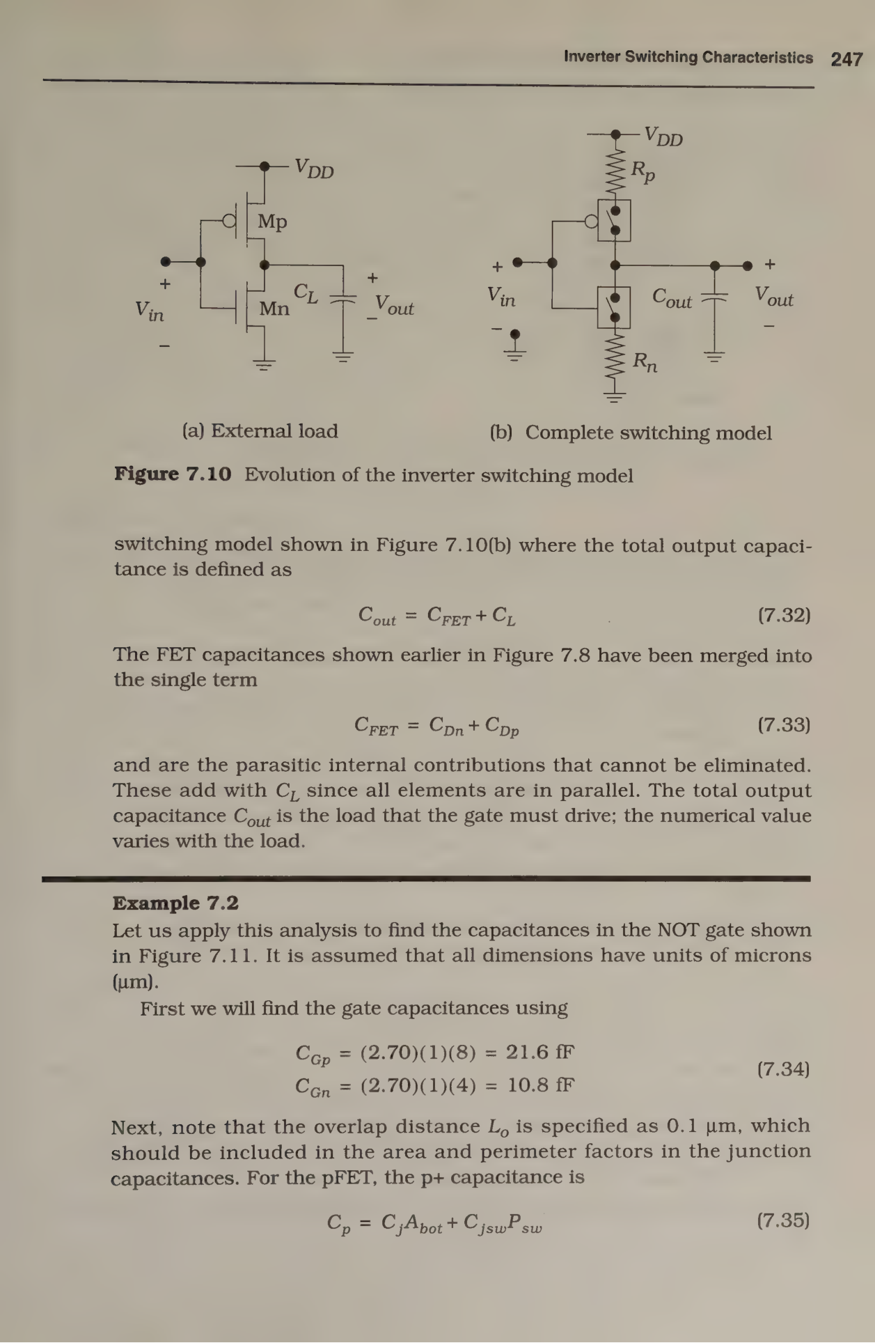
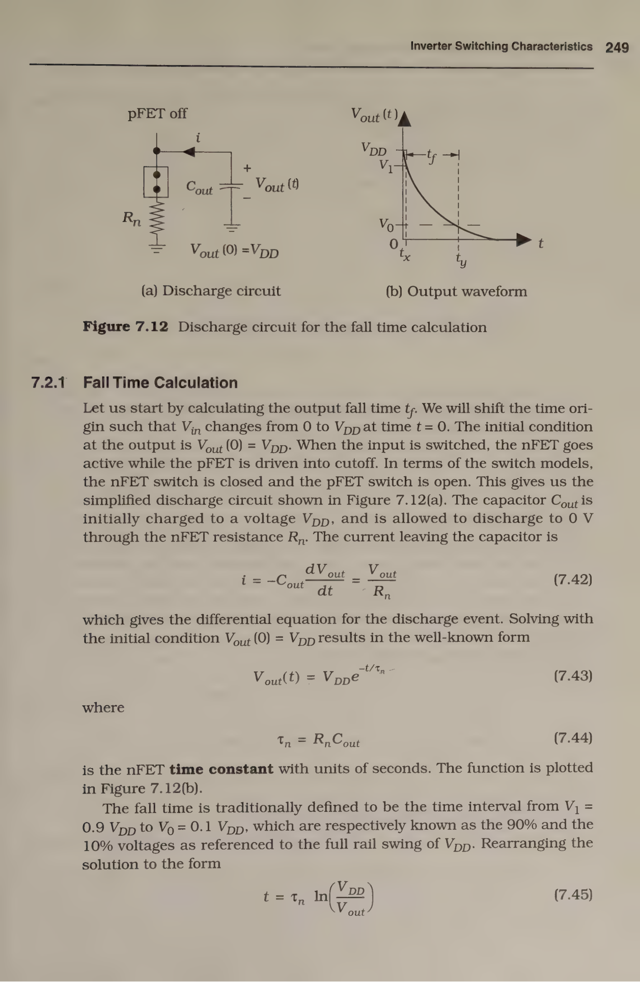
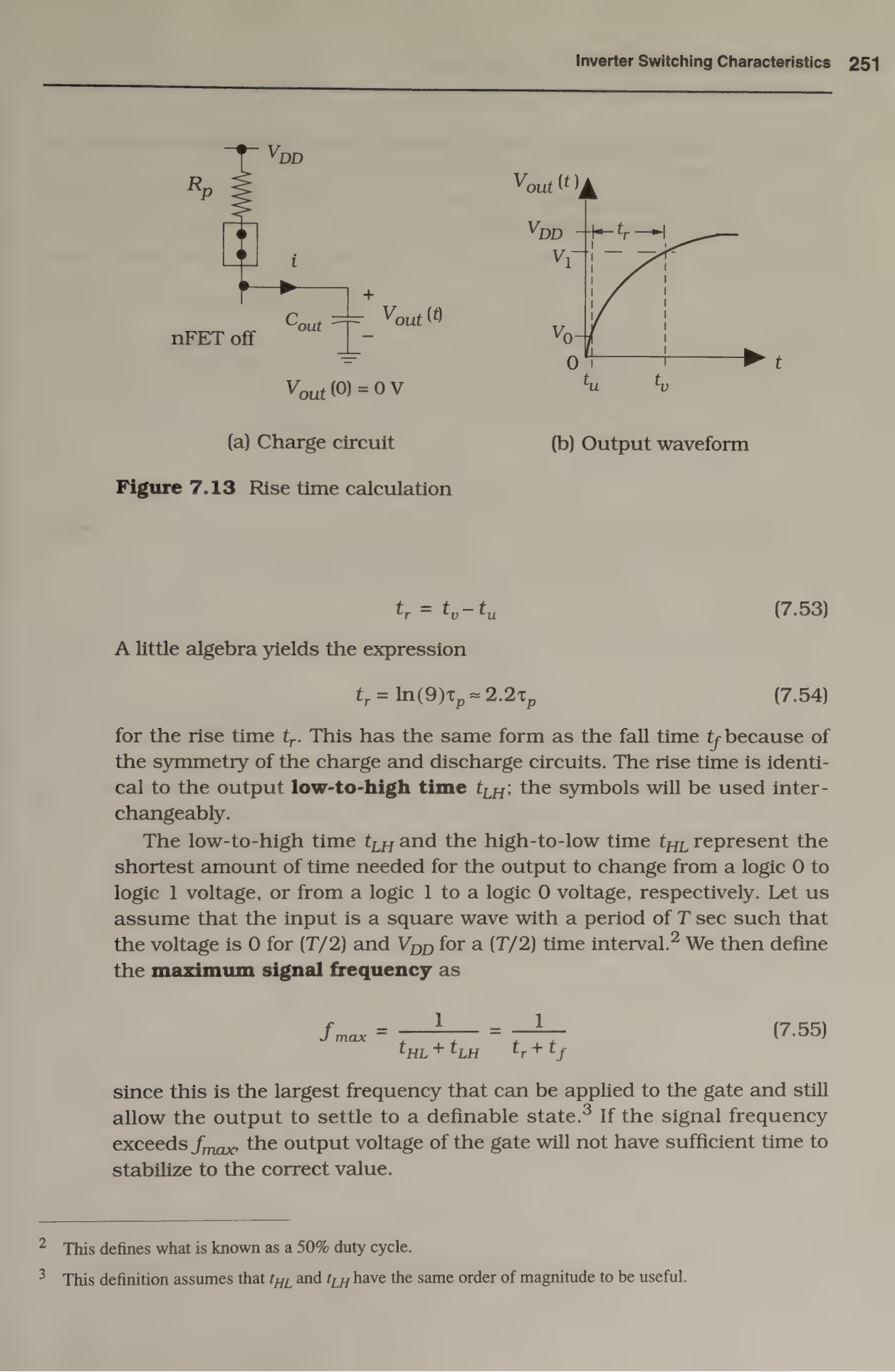
Cin=Cgn+Cgp (7.30) · CL=FO·Cin (7.31)
Cout=Cpar+CL, Cpar=Cdbn+Cdbp (7.32–7.33) ⭐
fmax=1/(tr+tf) (7.55) · tp=(tPHL,50%+tPLH,50%)/2, each 50% = ln2·τ≈0.69τ (7.64–7.66)
tr0=2.2RpCpar, tf0=2.2RnCpar (7.70) · αr=2.2Rp, αf=2.2Rn (7.71–7.72)
Symmetric (tr=tf): Rn=Rp → βn=βp if thresholds equal (7.81–7.84)
✅ Solved 7.2A — Ex 7.3 style (exam template)
Given: (W/L)n=6,(W/L)p=8, k′n=150,k′p=62 µA/V², VTn=0.7,|VTp|=0.85, VDD=3.3, Cout=150 fF.
βp=62·8=496 µA/V². Rp=1/[496e-6·(3.3−0.85)]=1/1.215e-3=822.9 Ω. τp=822.9·150e-15=123.4 ps. tr=2.2·123.4=271.6 ps.
βn=150·6=900 µA/V². Rn=1/[900e-6·2.6]=427.4 Ω. τn=64.1 ps. tf=141.0 ps. fmax=1/(412.6ps)=2.42 GHz.
Note asymmetry (tr>tf) because pFET weaker — exactly what symmetric sizing fixes.
✏️ Try yourself 7.2B (Problem [7.3] c–d)
βn=2.1 mA/V², βp=1.8 mA/V², VTn=0.6, VTp=−0.7, VDD=5, Cpar=74 fF. (a) VM? (b) Rn,Rp? (c) tr,tf at CL=0? (d) at CL=115 fF?
Answers: (a) √(2.1/1.8)=1.08 → VM=(5−0.7+1.08·0.6)/2.08=(4.3+0.648)/2.08=2.38 V. (b) Rn=1/[2.1e-3·4.4]=108 Ω, Rp=1/[1.8e-3·4.3]=129 Ω. (c) tf0=2.2·108·74f=17.6 ps, tr0=2.2·129·74f=21.0 ps. (d) Cout=189 fF → tf=2.2·108·189f=44.9 ps, tr=53.6 ps.
7.3 Power Dissipation (pp.257–260)
Shortest section, 1 numerical. Derivation = charge per cycle.
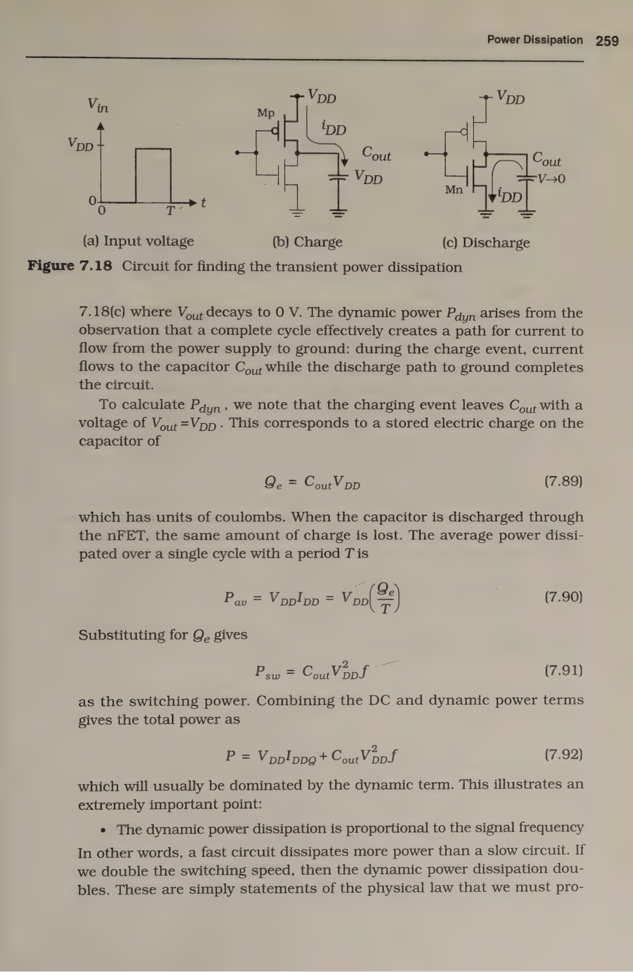
PDC=VDDIDDq (leakage ~pA) (7.87)
Qc=CoutVDD (7.89) → Pav=VDD(Qc/T) (7.90)
✅ Solved 7.3A
Cout=100 fF, VDD=5, f=100 MHz, IDDq=10 pA. Pdyn=100e-15·25·1e8=250 µW. PDC=5·10e-12=50 pW. Total≈250 µW (dynamic 10⁷× bigger).
At 1 GHz → 2.5 mW. For 1 mW need f=1e-3/(100e-15·25)=400 MHz.
✏️ Try yourself 7.3B
Cout=80 fF, VDD=3.3 V, f=500 MHz. Find Pdyn. Ans: 80e-15·10.89·5e8 = 435.6 µW. If VDD scaled to 2.0 V, new P? Ans: ×(2/3.3)²=0.367 → 160 µW. (Why voltage scaling matters!)
7.4 DC Characteristics: NAND and NOR Gates (pp.260–266)
Same VM trick with effective β. Remember direction of shift.
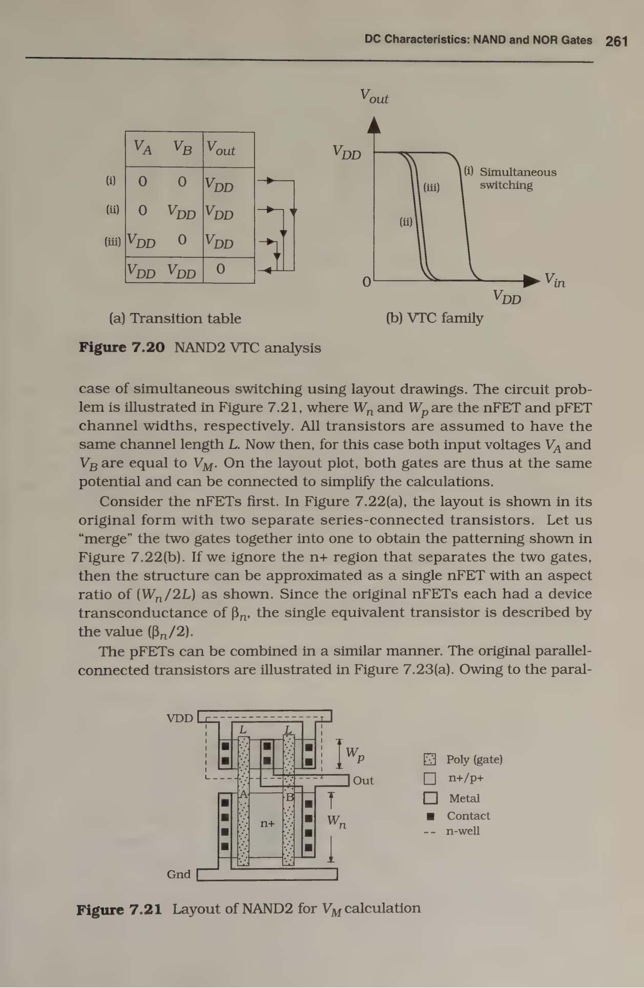
• NAND2 simultaneous (VA=VB): series nFETs ≈ one (Wn/2L) → βn,eff=βn/2; parallel pFETs ≈ one (2Wp/L) → βp,eff=2βp. Plug into 7.14 with √(βn,eff/βp,eff)=(1/2)√(βn/βp).
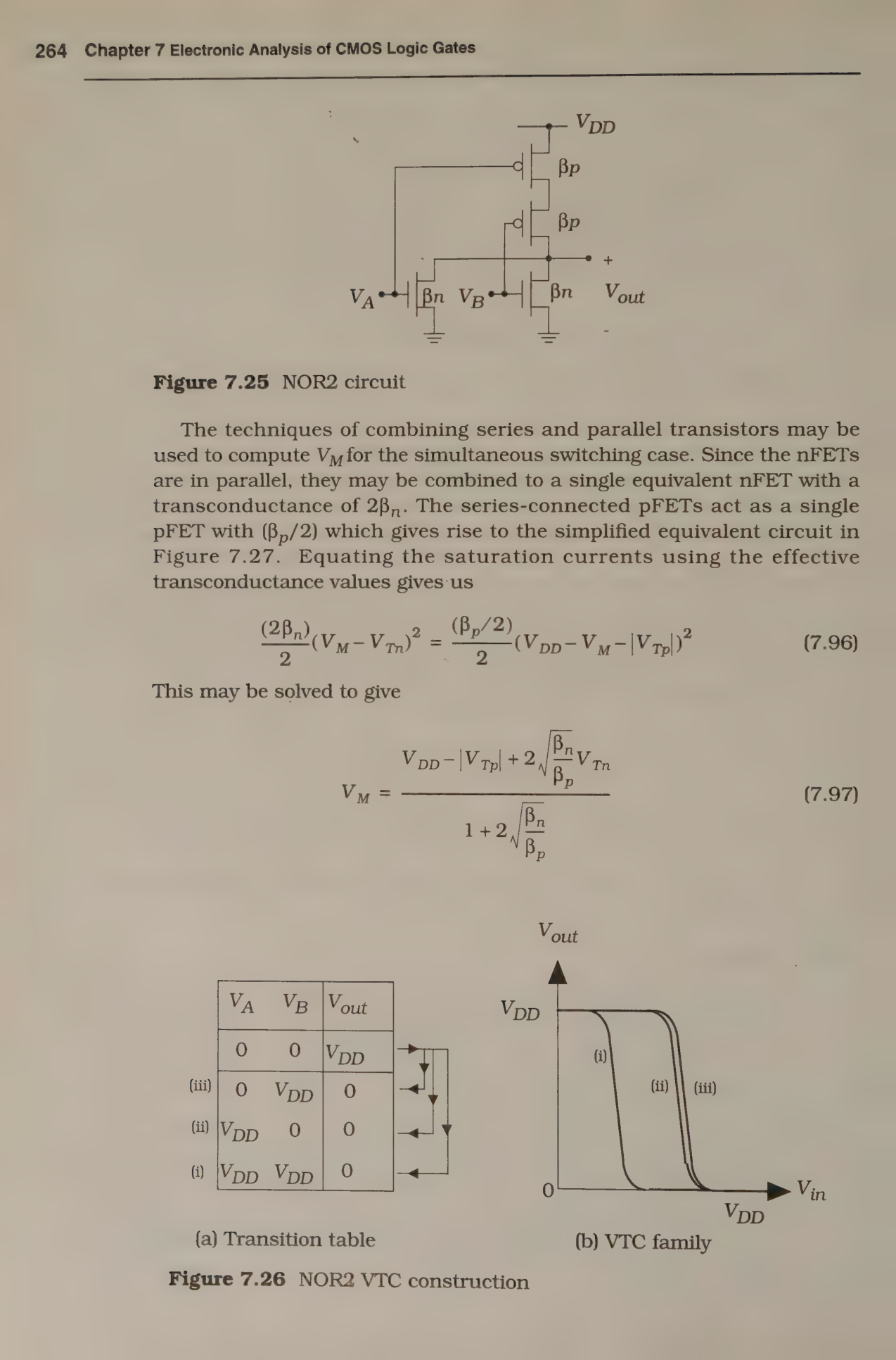
• NOR2 simultaneous: parallel n → 2βn; series p → βp/2 → factor 2√(βn/βp).
• N-input: NAND factor (1/N), NOR factor (N).
VM,NAND-N: replace ½ by 1/N (7.95)
VM,NOR2-sim = [VDD−|VTp| + 2√(βn/βp)·VTn]/[1+2√(βn/βp)] (7.97) ⭐
VM,NOR-N: replace 2 by N (7.98)
✅ Solved 7.4A — Problem [7.7] style
NAND2, βn=2βp (ratio 2, √=1.414), VDD=5, VTn=0.6, |VTp|=0.7.
Inverter: VM=(5−0.7+1.414·0.6)/2.414=(4.3+0.849)/2.414=2.13 V.
NAND2-sim: eff √=0.707. VM=(4.3+0.707·0.6)/1.707=(4.3+0.424)/1.707=2.77 V (+0.64 right shift ✓).
✏️ Try yourself 7.4B — Problem [7.8]
NOR2, βp=2.2βn → βn/βp=1/2.2=0.4545, √=0.674. VDD=3.3, VTn=0.65, |VTp|=0.8. Find simultaneous VM.
Ans: factor 2·0.674=1.348. VM=(3.3−0.8+1.348·0.65)/(1+1.348)=(2.5+0.876)/2.348=1.44 V. Inverter with same FETs would be (2.5+0.438)/1.674=1.755 V → left shift ✓.
7.5 NAND and NOR Transient Response (pp.266–272)
Worst-case philosophy + Elmore ladder. Draw subcircuits.
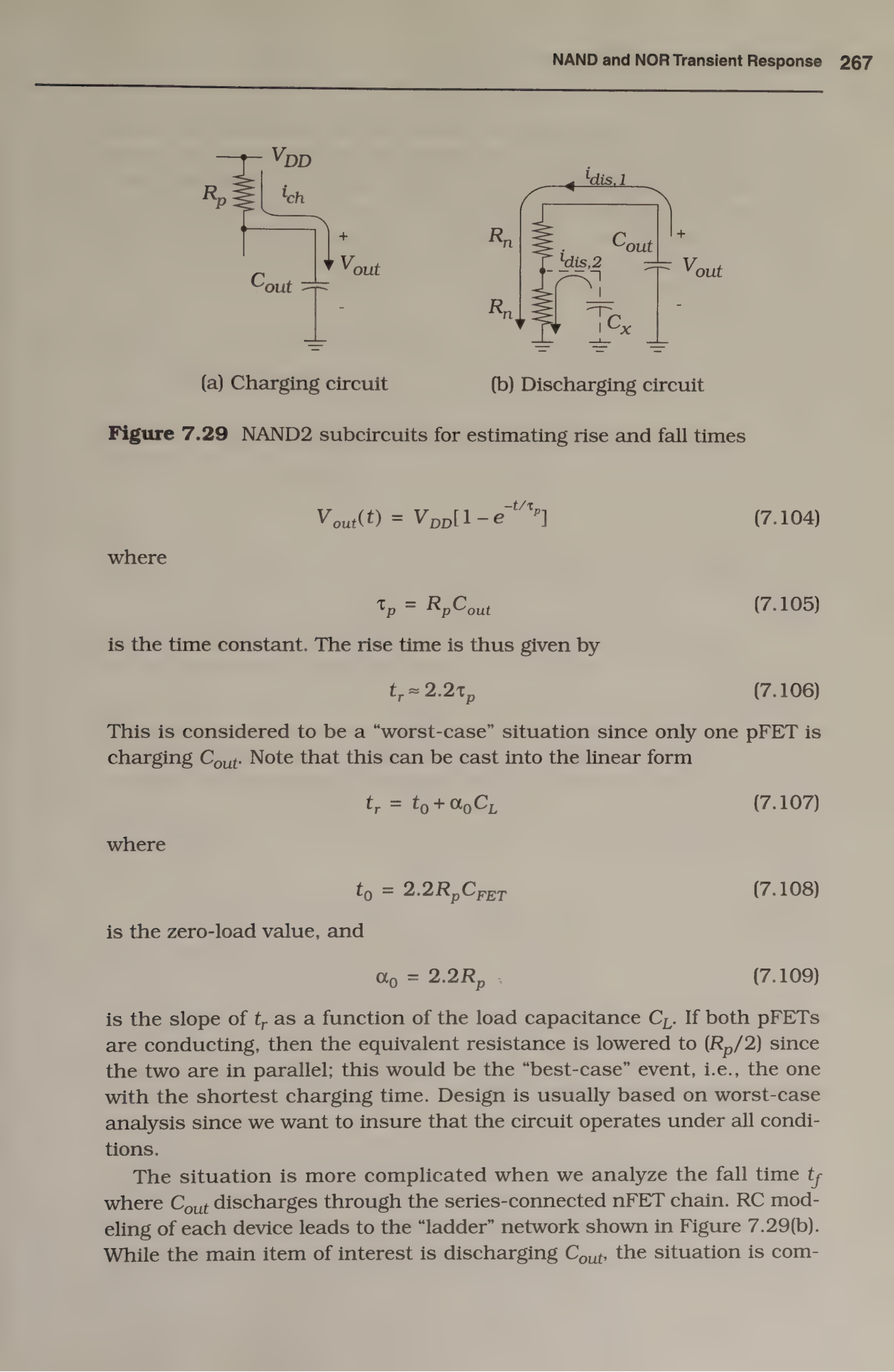
Rise (worst, 1 pFET): τp=RpCout, tr=2.2τp, tr0=2.2RpCpar, αr=2.2Rp (7.105–7.109)
tf=2.2τn, tf0=2.2Rn(2Cpar+Cx), αf=4.4Rn (doubled!) (7.115–7.119)
NOR2 rise (series): τp=Cout·2Rp+Cy·Rp, αr=4.4Rp (7.131–7.138) ⭐
✅ Solved 7.5A — comparison (viva favourite)
Rn=1k, Rp=2k, Cout=80 fF, Cx=Cy=10 fF.
NAND rise: τ=2k·80f=160ps→tr=352ps. NAND fall: τ=80f·2k+10f·1k=170ps→tf=374ps (balanced).
NOR fall: τ=1k·80f=80ps→tf=176ps. NOR rise: τ=80f·4k+10f·2k=340ps→tr=748ps (skewed! series-p is worst because Rp already 2×Rn). Conclusion: prefer NAND, limit p-stacks.
✏️ Try yourself 7.5B — Problem [7.10]
NAND3 chain: Cout=130 fF, C1=C2=36 fF, βn=2.0 mA/V², VDD=3.3, VTn=0.6. (a) Elmore τ with internals? (b) ignoring C1,C2? %error?
Ans: Rn=1/[2e-3·2.7]=185 Ω. Ladder top→GND: τ=Rn(C1+C2+Cout)+Rn(C2+Cout)+Rn·Cout? For 3-stack discharging down: τ=Rn·C1′+… Standard: τ=185·(36+36+130)+185·(36+130)+185·130 =185·(202+166+130)=185·498=92.1 ps. Ignoring internals: τ=3·Rn·Cout? ≈185·3·130? No — Cout only through 3R: τ=3·185·130f=72.2 ps. Error=(92.1−72.2)/92.1=21.6% under-estimate. (Method matters more than exact number — show Elmore sum.)
7.6 Analysis of Complex Logic Gates (pp.272–276)
Same method on AOI/OAI. Plus activity factor α.
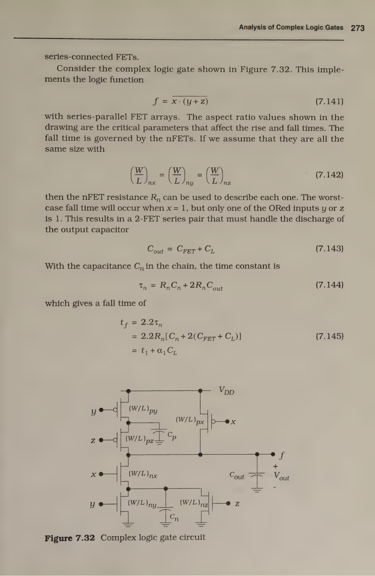
τp=Cout·2Rp+Cy·Rp, tr=tr0+αrCL (7.149–7.152)
αNOR2=αNAND2=3/16 (7.157–7.158) · αNOR3=7/64 (7.159) · αXNOR2=1/4 (7.160)
✅ Solved 7.6A — activity
NOR2, equiprobable inputs: P(out=0)=3/4 (only 00 gives 1), P(out=1)=1/4. α=3/4·1/4=3/16=0.1875. So Pdyn is only 18.75% of C·V²·f — big saving vs always-switching clock. XNOR2: P0=P1=1/2 → α=1/4.
7.7 Gate Design for Transient Performance (pp.276–281)
Design for speed first, check DC after. Reference = inverter.
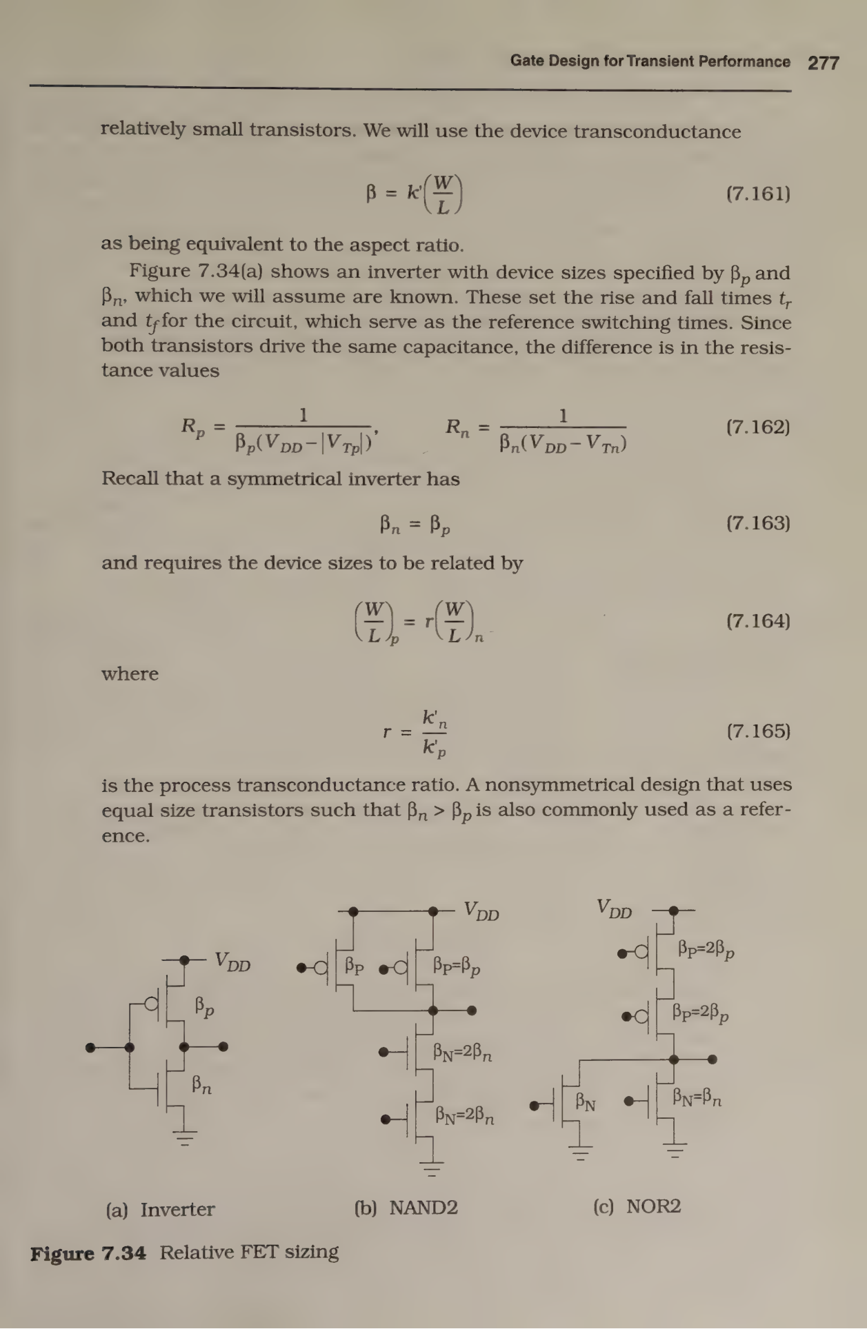
NOR2: βn(each)=βn,inv (1×); βp(each)=2·βp,inv (2×) (7.173–7.176) ⭐
NAND3: n 3×, p 1×; NOR3: n 1×, p 3× (7.177–7.180) · General: n-series → n×
✅ Solved 7.7A
k′n/k′p=2.5, inv (W/L)n=2. Symmetric → (W/L)p=2.5·2=5. NAND2: p each=5 (1×), n each=2·2=4 (2×). NOR2: n each=2, p each=2·5=10. Note NOR pFETs huge — reason NAND preferred.
✏️ Try yourself 7.7B — Problems [7.11]–[7.13] pattern
F=a·b+c·d·e (AOI). Inv ref βn=βp. Size for equal R? Ans: Longest n-discharge = 3 series? (c·d·e) → all n 3×. Worst p-charge = 2 series (a,b side + c,d side in dual) → those p 2×, solo p 1× (or 2× uniform). Draw both arrays to justify.
7.8 Transmission Gates and Pass Transistors (pp.281–285)
No rail → no restoration → threshold drop. Favourite short-note Q.
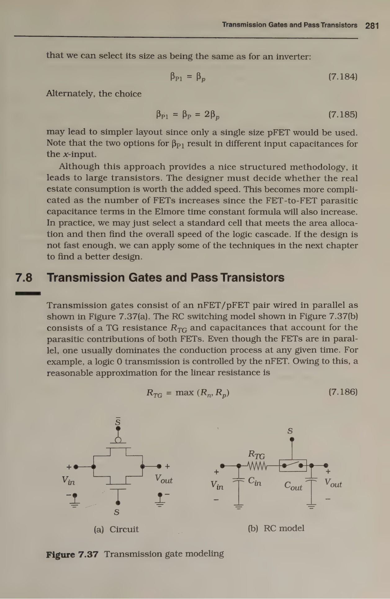
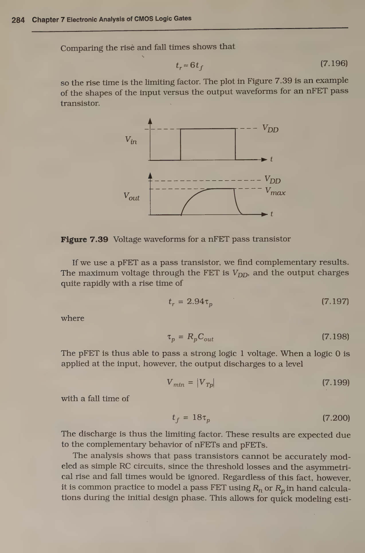
tr=18τn (0→0.9Vmax, rational not exponential) (7.192) · tf≈2.94τn (clean to 0) (7.195) · tr≈6tf (rise-limited) (7.196)
✅ Solved 7.8A — Problems [7.14]/[7.15] style
VDD=5, VTn=0.5, βn=1.5 mA/V², Cout=84 fF, logic-1 in, cap empty. Rn=1/[1.5e-3·4.5]=148 Ω. τn=148·84f=12.4 ps. tr=18·12.4=224 ps to 0.9·4.5 V. Vmax=4.5 V. Switch to 0: tf=2.94·12.4=36.5 ps. Ratio ≈6 ✓.
pFET: W/L=8, k′p=60µ, VDD=3.3, |VTp|=0.8, Cout=50 fF, cap at VDD→in 0. βp=480µ, Rp=1/[480e-6·2.5]=833 Ω, τp=41.7ps. Fall (limited, to |VTp|): slow; rise back: tr=2.94·41.7=122.5 ps.
7.9 Comments on SPICE Simulations (pp.285–288) — viva only
No numerical. Know 4 commands + 1 example.
- Why simulate: hand calcs use square-law + step input + voltage-independent C — estimates only. Tape-out needs SPICE (watch convergence/noise).
- Netlist: M1 D G S B MODEL W= L=, order Drain-Gate-Source-Bulk. Add AD/PD/AS/PS (area/perim) by hand if extractor omits.
- Sources: PULSE(V1 V2 TD TR TF PW PER), EXP(...). Analyses: .DC VIN 0 VDD STEP (VTC), .TRAN TSTEP TSTOP.
- Ex 7.5: shared 10×8 region (A=80, P=36) split e.g. AS=40P/PS=18U + AD=40P/PD=18U (equal) or 10/70 split — both valid if totals ≤ real.
📋 Master formula sheet (print this — 1 page)
All equations with book numbers. Revise by covering right column.
| # | Formula (what to write) | When / meaning |
|---|---|---|
| 7.1–7.3 | VOH=VDD, VOL=0, VL=VDD | Full-rail endpoints |
| 7.8 | NML=VIL−VOL, NMH=VOH−VIH | Noise margins (slope −1 pts) |
| 7.14 ⭐ | VM=[VDD−|VTp|+√(βn/βp)·VTn]/[1+√(βn/βp)], β=k′(W/L) | Inverter threshold — #1 asked |
| 7.20 | Symmetric (VTn=|VTp|): βn=βp → Wp/Wn=k′n/k′p≈2–3 | Centred VTC |
| 7.28 ⭐ | Rn=1/[βn(VDD−VTn)], Rp=1/[βp(VDD−|VTp|)] | FET resistors |
| 7.32 | Cout=Cpar+CL, Cpar=Cdbn+Cdbp | Total load |
| 7.48/54 ⭐ | tf≈2.2RnCout, tr≈2.2RpCout | 90–10% times |
| 7.55 | fmax=1/(tr+tf) | Max toggle |
| 7.65–66 | t50%=0.69τ, tp=(tPHL50+tPLH50)/2 | Prop delay |
| 7.69–72 | tr=tr0+αrCL, tf=tf0+αfCL; tr0=2.2RpCpar; αr=2.2Rp (same f) | Load sweep |
| 7.91–92 ⭐ | Pdyn=CoutVDD²f, P=PDC+Pdyn, PDC=VDDIDDq | Power |
| 7.94/95 | VM,NAND: √(·)→(1/N)√(βn/βp) — shifts RIGHT | NAND DC |
| 7.97/98 | VM,NOR: √(·)→N√(βn/βp) — shifts LEFT | NOR DC |
| 7.111 | NAND fall: τn=Cout·2Rn+Cx·Rn, αf=4.4Rn | Series-n delay |
| 7.134 | NOR rise: τp=Cout·2Rp+Cy·Rp, αr=4.4Rp | Series-p delay |
| 7.154 | Pdyn=αCV²f; αNOR2=3/16, αXNOR=1/4 | Activity |
| 7.171–176 | NAND: n 2× p 1×; NOR: n 1× p 2×; N-in: series N× | Sizing |
| 7.186–196 | RTG=max(Rn,Rp); n-pass Vmax=VDD−VTn, tr=18τn, tf=2.94τn, tr≈6tf | TG/pass |
📝 Numerical bank — solved + exam drills (with textbook problems verbatim)
Do solved first (answers open), then closed-book drills. Problems [7.x] are verbatim from pp.288–291.
A. Solved drills (one per section — done above, quick links)
- 7.1A (VM/sizing), 7.2A (tr/tf/fmax), 7.3A (power), 7.4A (NAND shift), 7.5A (NAND vs NOR), 7.6A (α), 7.7A (sizing), 7.8A (pass FET) — all with full steps above. Re-solve each in <5 min.
B. Textbook problems — attempt these (starred = your listed Exercises 2,3,5,6,14,15)
[7.2] ⭐, [7.3] ⭐, [7.5] ⭐, [7.6] ⭐, [7.14] ⭐, [7.15] ⭐ + rest — click to see full statements & hints
[7.1] k′n=100µ, VTn=0.70, k′p=42µ, VTp=−0.60, VDD=3.3, (W/L)n=10,(W/L)p=14. Find VM. → 7.14 direct.
[7.2] ⭐ (your Ex-2) Find βn/βp for VM=1.3 V, VDD=3 V, VTn=0.6, VTp=−0.82. Relative sizes if k′n=110µ, µp=µn/2.2? Hint: invert 7.14: √(βn/βp)=(VDD−VM−|VTp|)/(VM−VTn). Ans: √=(3−1.3−0.82)/(1.3−0.6)=0.88/0.7=1.257→ratio=1.58.
[7.3] ⭐ (your Ex-3) βn=2.1m, βp=1.8m, VTn=0.6, VTp=−0.7, VDD=5, Cpar=74f. (a) VM (b) Rn,Rp (c) tr,tf at CL=0 (d) at CL=115f (e) plot vs CL. → solved 7.2B above.
[7.4] VM for Fig 7.11 layout. → extract (W/L) from layout, apply 7.14.
[7.5] ⭐ (your Ex-5) Fig 7.11 + CL=80f, Lelec=0.8µm. (a) Cin (b) Rn,Rp (c) tr,tf. → Cin=Cg sum; R via 7.28; t via 2.2RC.
[7.6] ⭐ (your Ex-6) SPICE Fig 7.11, CL=100f, DC+transient. → deck in 7.9; compare VM/tr with hand calc.
[7.7] NAND2 βn=2βp, VDD=5, VTn=0.6, VTp=−0.7. (a) simultaneous VM (b) inverter VM same β. → solved 7.4A.
[7.8] NOR2 βp=2.2βn, VDD=3.3, VTn=0.65, VTp=−0.8. Simultaneous VM. → try 7.4B.
[7.9] NAND3 n W/L=4 each, k′n=120µ, VTn=0.55, VDD=5, want simultaneous VM=2.4, VTp=−0.9, r=2.4. Find βp. Hint: 7.95 with N=3, solve for √(βn/βp).
[7.10] NAND3 chain Cout=130f, C1=C2=36f, βn=2m, VDD=3.3, VTn=0.6. Elmore τ? Ignore C1,C2? %error? → try 7.5B.
[7.11]–[7.13] Complex sizing (AOI/OAI: F=a·b+c·d·e etc.). → method in 7.6/7.7: longest chain → n×.
[7.14] ⭐ (your Ex-14) n-pass βn=1.5m, VDD=5, VTn=0.5, Cout=84f, uncharged. (a) τ (b) tr (c) switch to 0: tf (d) SPICE. → solved 7.8A: τ=12.4ps, tr=224ps, tf=36.5ps.
[7.15] ⭐ (your Ex-15) p-pass W/L=8, k′p=60µ, VDD=3.3, VTp=−0.8, Cout=50f, cap at VDD→in 0. (a) tf (b) back to VDD: tr. → solved 7.8A: tr≈122ps, fall limited to |VTp|.
C. 5-min mock (closed book — predict your quiz)
Q2 (4m): Same inverter, Cout=200fF. Find Rn,Rp,tr,tf,fmax.
Q3 (2m): NAND2 with same FETs — simultaneous VM? Left or right of inverter? Why? + Pdyn if Cout=200f,VDD=3,f=200MHz.
Check answers
Q1: βn=480µ,βp=300µ,ratio=1.6,√=1.265,VM=(3−0.7+1.265·0.6)/2.265=(2.3+0.759)/2.265=1.35V. Symmetric: Wp/Wn=120/50=2.4 → need (W/L)p=2.4·4=9.6.
Q2: Rn=1/[480e-6·2.4]=868Ω, Rp=1/[300e-6·2.3]=1449Ω. τn=173.6ps→tf=382ps; τp=289.9ps→tr=638ps; fmax=0.98GHz.
Q3: eff√=0.632,VM=(2.3+0.632·0.6)/1.632=1.64V (right of 1.35 ✓ series-n). Pdyn=200e-15·9·2e8=360µW.
⚠️ Traps & final checklist
1. VDD vs Vpp same; |VTp| positive in formulas (don't plug −0.7).
2. β=k′(W/L) — multiply BEFORE ratio, watch µA→A (×1e-6).
3. tr uses Rp, tf uses Rn (crossed!).
4. 2.2 for 10–90%, 0.69 for 50% — don't swap.
5. NAND→right, NOR→left (simultaneous). Parallel=1×, series=n×.
6. Pass FET: n can't pass 1 (Vmax=VDD−VTn, tr=18τ); p can't pass 0 (Vmin=|VTp|).
☐ Write 7.14 from memory
☐ Write 7.28 + 2.2/0.69
☐ Write Pdyn + sizing rules
☐ Re-solve 7.1A + 7.2A without peeking
☐ Read all figure captions once
☐ Sleep — VM shifts are easy marks when fresh.
Sources: all equations/derivations/figures from Uyemura Ch.7 pp.237–288 (PDF pp.253–305). Page renders in ch7_figs/ are full textbook pages — zoom to read fine print. Course Plan: 23ECE302 Unit II (Lec 20–28). Good luck! ⚡